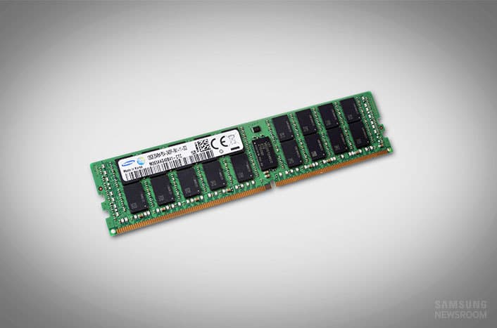
Samsung Electronics announced that it has begun mass producing the industry’s first 4-gigabyte (GB) DRAM package based on the second-generation High Bandwidth Memory (HBM2) interface, for use in high performance computing (HPC), advanced graphics and network systems, as well as enterprise servers. Based on the HBM solution this will make the DRAM perform – more than seven times faster than the current DRAM performance limit which will ultimately allow for faster responsiveness in high-end computing tasks including parallel computing, graphics rendering and machine learning.
“By mass producing next-generation HBM2 DRAM, we can contribute much more to the rapid adoption of next-generation HPC systems by global IT companies,” said Sewon Chun, senior vice president, Memory Marketing, Samsung Electronics. “Also, in using our 3D memory technology here, we can more proactively cope with the multifaceted needs of global IT, while at the same time strengthening the foundation for future growth of the DRAM market.”
The newly introduced 4GB HBM2 DRAM, which uses the company’s 20-nanometer process technology and advanced HBM chip design, suits the need for high performance, energy efficiency, reliability and small dimensions demanded by the next-generation HPC systems and graphics cards.
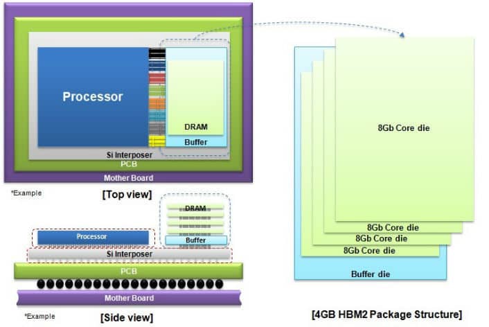
According to the official news site, the 4GB HBM2 package is created by stacking a buffer die at the bottom and four 8-gigabit (Gb) core dies on top. These are then vertically interconnected by TSV holes and microbumps. A single 8Gb HBM2 die contains over 5,000 TSV holes, which is more than 36 times that of a 8Gb TSV DDR4 die, offering a dramatic improvement in data transmission performance compared to typical wire-bonding based packages.
The result is a 256GBps of bandwidth, which is double that of a HBM1 DRAM package which is equivalent to more than seven-fold increase over the 36GBps bandwidth of a 4Gb GDDR5 DRAM chip, that currently has the fastest data speed per pin (9Gbps) among manufactured DRAM chips today. The new DRAMS also enables enhanced power efficiency by doubling the bandwidth per watt over a 4Gb-GDDR5-based solution, and embeds ECC (error-correcting code) functionality to offer high reliability.
In addition, Samsung plans to produce an 8GB HBM2 DRAM package within this year fitted in graphics cards, designers will be able to enjoy space savings of more than 95 percent, compared to using GDDR5 DRAM, offering more optimal solutions for compact devices that require high-level graphics computing capabilities, the firm when on to add.