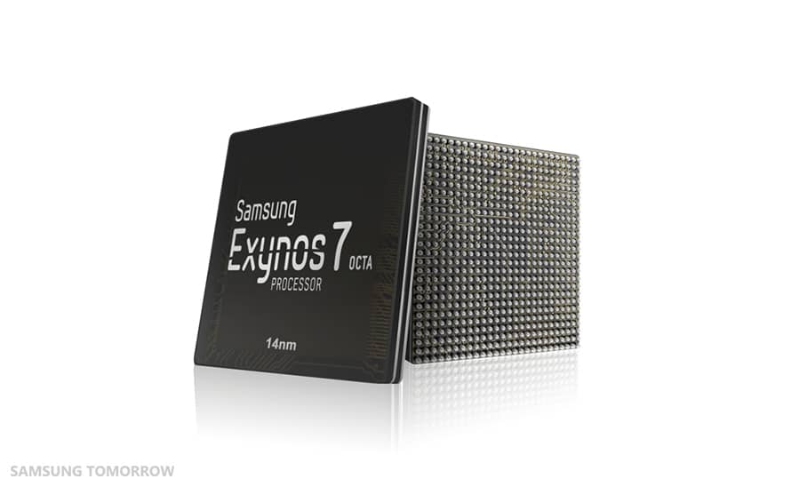
Samsung Electronics has announced that it has begun mass production of advanced logic chips utilizing its 14nm LPP(Low-Power Plus) process, the 2nd generation of the company’s 14nm FinFET process technology. Early last year the semi conductor firm also announced the launch of the Exynos 7 Octa processor built on the industry’s first 14nm LPE (Low-Power Early) process. With the new 14nm LPP process, its many customers including Qualcomm Technologies will be using the chips for their Snapdragon 820 processor and is scheduled to be in devices in the first half of this year.
“We are pleased to start production of our industry-leading, 2nd generation 14nm FinFET process technology that delivers the highest level of performance and power efficiency” said Charlie Bae, Executive Vice President of Sales & Marketing, System LSI Business, Samsung Electronics. “Samsung will continue to offer derivative processes of its advanced 14nm FinFET technology to maintain our technology leadership.”
Incorporating three-dimensional (3D) FinFET structure on transistors enables significant performance boost and low power consumption. Samsung’s new 14nm LPP process delivers up to 15 percent higher speed and 15 percent less power consumption over the previous 14nm LPE process through improvements in transistor structure and process optimization. In addition, use of fully-depleted FinFET transistors brings enhanced manufacturing capabilities to overcome scaling limitations.
With its characteristics, 14nm FinFET process is considered to be one of the most optimised solutions for mobile and IoT applications and is expected to meet growing market demand for a wide range of high performance and power efficient applications from network to automotive.